
English 
T: +86-571-8663-6649
E: hzbjys@hzbjys.com
E: hzbjys@hzbjys.com
7/F, 1st Building Of ZhongHao WangJiang International Center, NO.332 East WangJiang Road, HangZhou, ZheJiang, China.
Views: 0 Author: Site Editor Publish Time: 2026-07-30 Origin: Site


Selecting the correct copper profile determines your fabrication methodology, environmental durability, and final product viability. Mis-specifying material thickness introduces severe engineering risks on the shop floor. Using a thin profile where heavy mass is required leads to structural failure under load and dangerous thermal bottlenecks. Conversely, over-specifying thickness causes excessive material waste and machining inefficiencies during high-volume production runs.
Engineers and fabricators must understand exact dimensional thresholds to optimize performance. Material selection directly impacts mechanical properties and application-specific criteria. This evaluation framework breaks down the technical differences between thin and thick copper profiles. We will detail how to match specific alloy tempers, fabrication methods, and thermal requirements to the correct material format, ensuring structural integrity without over-engineering.
Dimensional Thresholds: The industry-standard dividing line between sheet and plate is typically 0.188 inches (3/16")—materials below this are sheets, while those above are plates.
Formability vs. Rigidity: Copper sheet offers superior hot and cold-working capabilities for intricate forming, whereas copper plate provides the structural integrity required for heavy-duty machining and load-bearing.
Application Specificity: Copper sheet is the standard for high-precision electrical routing (e.g., PCBs) and architectural flashing, while plate is reserved for heavy busbars, heat exchangers, and industrial molds.
Durability and Yield: Material selection must balance raw weight costs and machining time against the required service life, leveraging copper's naturally low reactivity to water and acids.
Establishing a standardized baseline for material specification ensures accurate vendor communication. Procurement errors often stem from confusing industry measurement systems. Clear definitions prevent costly delays on the shop floor and ensure you receive the exact material required for your fabrication process.
The exact dimensional cutoff between these two formats is 0.188 inches, which equals 4.76 millimeters or 3/16 of an inch. Materials falling below this specific measurement classify as sheets. Materials measuring at or above this line classify as plates. This standard applies across primary metal suppliers and fabrication facilities.
Measurement conventions shift depending on the format. Fabricators measure thin profiles using the gauge system or mils. The American Wire Gauge (AWG) system frequently applies to non-ferrous metals. One mil equals one-thousandth of an inch (0.001"). In contrast, fabricators measure thick profiles using fractional inches or exact millimeters. This distinction requires careful attention during the drafting phase to avoid ordering material that is ten times too thick or too thin.
Copper foil represents a distinct category, measuring under 0.005 inches. The practical transition point from foil to standard sheet occurs around 10 mil (0.010 inches). Below 10 mil, the metal behaves like fragile paper. It tears easily and requires specialized roll-to-roll handling equipment. At 10 mil and above, the material assumes durable, workable characteristics. It holds its shape under its own weight and supports standard fabrication techniques like shearing and punching.
Standard Copper Thickness Measurement Conversions
Material Classification | AWG Gauge | Decimal Inches | Millimeters |
|---|---|---|---|
Foil | N/A | 0.005" | 0.127 mm |
Sheet (Thin) | 30 AWG | 0.010" | 0.254 mm |
Sheet (Medium) | 16 AWG | 0.050" | 1.290 mm |
Sheet (Thick) | 8 AWG | 0.128" | 3.260 mm |
Plate (Threshold) | N/A | 0.188" (3/16") | 4.760 mm |
Plate (Heavy) | N/A | 0.500" (1/2") | 12.700 mm |
Both formats share common high-purity alloy grades, but their availability in specific tempers varies. C11000 Electrolytic Tough Pitch (ETP) remains the most common choice for general electrical and architectural work. It offers 100% IACS conductivity but contains trace amounts of oxygen. C10100 Oxygen-Free Electronic (OFE) provides superior conductivity and prevents hydrogen embrittlement during high-heat brazing or welding. C12200 Phosphorus-Deoxidized High Residual Phosphorus (DHP) excels in plumbing and heavy welding applications where maximum electrical conductivity is not the primary goal.
Temper availability shifts dramatically based on the manufacturing process. Rolling mills produce thin profiles with highly controlled grain structures. This allows for specific tempers like H02 Half Hard or O60 Soft. Fabricators rely on O60 Soft for deep drawing and intricate stamping because it yields without tearing. Thick profiles often undergo casting followed by heavy hot rolling. Achieving a uniform H02 temper throughout a thick cross-section proves difficult. Therefore, heavy profiles often arrive in an as-hot-rolled or lightly annealed state, prioritizing bulk strength over precise malleability.
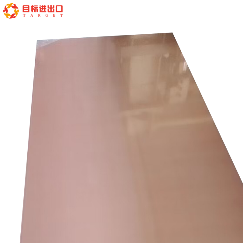
Thin copper profiles offer specific mechanical, thermal, and chemical advantages. Their high surface area and flexibility make them highly effective for precision engineering, electrical routing, and rapid thermal transfer applications.
Thin profiles excel in cold forming operations. Operators can bend, stamp, and deep-draw the metal without fracturing the grain structure. Cold working hardens the material, increasing its yield strength. When extensive forming is required, operators may need to pause and anneal the metal to restore ductility. Annealing copper requires heating it to between 700°F and 1200°F, followed by rapid quenching. Thin profiles require less frequent annealing compared to thicker sections and heat up much faster in the furnace.
Grain structure plays a critical role in directional strength. The rolling process elongates the metallic grains parallel to the rolling direction. Bending parallel to the grain increases the risk of cracking, especially on tight radii. Fabricators must orient flat patterns so that critical bends occur perpendicular to the grain direction. A standard rule of thumb on the shop floor is to maintain a minimum bend radius of 1T (one times the material thickness) for soft tempers, and up to 3T for harder tempers. This practice maximizes overall durability and prevents fatigue failures in vibrating environments.
The electronics industry relies heavily on copper sheet for pcb applications. Manufacturers utilize two primary types: electrodeposited (ED) and rolled-annealed (RA). ED copper forms via an electrolytic process, creating a vertical grain structure. This structure bonds exceptionally well to dielectric substrates like FR4. RA copper passes through heavy rollers, creating a horizontal grain structure. RA copper withstands repeated flexing, making it ideal for flexible printed circuits used in aerospace and consumer electronics.
Performance metrics dictate material selection for high-density interconnects. Peel strength measures the force required to separate the metal from the substrate. Surface roughness directly impacts this bond. A rougher surface increases mechanical adhesion but can disrupt high-frequency signal integrity due to the skin effect. Etching precision relies on uniform material density. Voids or impurities cause uneven etching, leading to short circuits or broken traces in dense circuit board layouts.
A high surface-area-to-volume ratio optimizes rapid heat dissipation. Electronics and HVAC fins utilize this property to shed thermal loads quickly. The thin cross-section allows heat to reach the surface rapidly, where forced air or liquid cooling carries it away. Copper Sheet outperforms thicker blocks in scenarios requiring rapid thermal transfer rather than thermal storage.
High-frequency electrical applications experience the skin effect. Alternating current tends to flow near the surface of the conductor. As frequency increases, the current is pushed further outward. At 1 MHz, the skin depth of copper is only about 0.0026 inches. The center of a thick conductor carries very little current at high frequencies. Thin profiles provide sufficient surface area for current carrying without adding excess mass. This keeps aerospace and telecommunications equipment lightweight while maintaining optimal electrical performance.
Thick-profile copper provides immense structural and thermal mass benefits. These properties suit extreme industrial environments where thin profiles would fail instantly under mechanical stress or thermal overload.
Heavy profiles deliver exceptional rigidity and tensile strength. Mechanical stress from heavy machinery or structural loads requires substantial material mass. While copper is inherently softer than steel, a thick cross-section provides sufficient resistance to bending and shearing forces. Engineers specify these profiles for heavy-duty switchgear components that must withstand the mechanical shock of high-voltage breaker operations.
Resistance to deformation proves critical in high-pressure environments. Vacuum chambers and cryogenic equipment subject materials to extreme pressure differentials. Thin profiles would buckle or implode under these conditions. Thick profiles maintain their dimensional stability, ensuring airtight seals and structural safety over decades of continuous operation. A one-inch thick block of C11000 copper provides a yield strength of roughly 10,000 to 11,000 psi in its annealed state, which is more than enough to handle heavy industrial clamping forces.
Fabrication methods contrast sharply based on material thickness. Thick profiles require heavy material removal. CNC milling, deep drilling, and rigid tapping dominate the workflow. Operators must manage tool deflection and chip evacuation carefully. In contrast, utilizing copper sheet for industrial fabrication relies on shearing, turret punching, and press brake forming. These methods move the metal rather than cutting it away, resulting in faster production times and less scrap.
Machining heavy copper presents unique tooling considerations. The metal is highly ductile and tends to gall, meaning it sticks to the cutting tool edges. This built-up edge ruins surface finishes and snaps end mills. Machinists must use sharp, polished, uncoated carbide tools with high positive rake angles. High feed rates combined with generous, high-pressure coolant flow prevent the metal from overheating and smearing during heavy milling operations. You cannot cut thick copper using the same speeds and feeds you would use for aluminum or mild steel.
Heavy profiles excel at absorbing and storing large thermal loads. Industrial heat exchangers, welding fixtures, and plastic injection molds require massive thermal mass. Copper has a specific heat capacity of 0.385 J/g°C. When a sudden spike in temperature occurs, a thick block absorbs the energy without a rapid rise in its own surface temperature.
This thermal buffering protects sensitive components from heat damage. In plastic injection molding, thick copper alloy inserts pull heat away from the plastic part rapidly and evenly. This reduces cycle times and prevents the plastic from warping as it cools. A thin profile would saturate with heat instantly and fail to cool the mold effectively.
Directly comparing these formats across critical engineering requirements clarifies the decision process. Each dimension impacts the final product's functionality and manufacturing viability.
Material Format Technical Comparison
Engineering Requirement | Thin Profile (< 0.188") | Thick Profile (≥ 0.188") |
|---|---|---|
Primary Fabrication Method | Stamping, bending, shearing, deep drawing | CNC milling, drilling, heavy waterjet cutting |
Thermal Function | Rapid heat dissipation (high surface area) | Thermal mass storage (high volume) |
Electrical Application | PCBs, high-frequency shielding, light traces | Heavy busbars, high-voltage switchgear |
Joining Techniques | Soldering, light brazing, spot welding | TIG/MIG welding, heavy mechanical fastening |
Weight per Square Foot | Lightweight (e.g., 16 AWG = 2.3 lbs/sq ft) | Heavyweight (e.g., 1/2" = 22.6 lbs/sq ft) |
Weight and raw material costs increase exponentially as thickness transitions past the 0.188-inch mark. Copper is a dense material, weighing approximately 0.323 pounds per cubic inch. Specifying a thick profile dramatically increases the weight of the final assembly. A 12x12x1-inch block weighs nearly 47 pounds. This impacts shipping, handling, and the structural requirements of the supporting framework. Raw material expenditure scales directly with weight.
Engineers must calculate the minimum required thickness to meet structural and electrical needs. Over-engineering wastes resources. Finite Element Analysis (FEA) helps determine stress concentrations. If a component only requires high conductivity on the surface, engineers might choose a thinner profile backed by a cheaper, rigid material like aluminum or steel, rather than using a solid heavy block.
Copper exhibits inherently low reactivity to water and non-oxidizing acids. This ensures a long service life in harsh environments. When exposed to the atmosphere, the metal develops a protective patina. This thin layer of copper carbonate and copper sulfate prevents further oxidation. Both formats share this chemical advantage, but their application environments differ.
Thin profiles serve well as weather-exposed architectural flashing. Roofers fold and shape the metal around chimneys and valleys to create waterproof seals. The material withstands decades of rain and snow. Conversely, a copper plate is necessary for heavy-duty chemical processing vats and marine components. These applications face constant abrasion and aggressive chemical attacks. The thick cross-section provides a sacrificial allowance, ensuring the vessel remains structurally sound even if slight surface degradation occurs over time.
Joining methods vary significantly based on mass. Thin profiles offer highly reliable solderability. Capillary action pulls solder into tight joints, creating strong electrical and mechanical bonds. Light brazing also works well, provided the operator controls the heat input to prevent warping or melting the base metal.
Thick profiles require TIG or MIG welding, or heavy mechanical fastening. Welding heavy copper presents severe challenges due to the heat sink effect. The massive thermal conductivity pulls heat away from the weld pool almost instantly. Welders must heavily preheat the entire block—often exceeding 1000°F—before striking an arc. They also typically use a helium-argon shielding gas mix to generate a hotter arc. Failure to preheat results in lack of fusion and porous, weak welds. Mechanical fastening via drilled and tapped holes often provides a more reliable and serviceable connection for heavy busbars.
Standard mill finishes differ between the two formats. Thin profiles often arrive with polished, brushed, or mirror finishes. The rolling process imparts a smooth, consistent surface ready for aesthetic applications or immediate PCB lamination. Thickness tolerances remain extremely tight, often within a few thousandths of an inch.
Thick profiles typically arrive with a rougher, as-rolled or as-cast finish. The surface may show scale or minor imperfections from the heavy manufacturing process. Flatness tolerances are looser. Fabricators often must perform secondary surface machining, such as fly cutting or surface grinding, to achieve the precise flatness required for mounting semiconductor heat sinks or creating vacuum seals.
Handling and processing these materials on the shop floor introduces specific challenges. Proactive risk mitigation prevents scrap and maintains production schedules.
Thin profiles are highly susceptible to physical damage. Careless handling causes permanent creasing, edge dents, and surface scratches. Exposure to humidity accelerates surface oxidation, which ruins solderability and aesthetic finishes. To mitigate these risks, facilities must require PVC masking on all polished surfaces. Workers must wear clean cotton gloves to prevent transferring corrosive skin oils. Storage areas must remain climate-controlled with low humidity.
Thick profiles suffer from internal residual stresses generated during the manufacturing process. When a CNC machine removes a large volume of material from one side, these stresses release unevenly. The block will warp or bow, destroying dimensional accuracy. To mitigate this, engineers must specify stress-relieved material for high-tolerance machining. Machinists should also utilize balanced roughing toolpaths, removing equal amounts of material from both sides before taking final finishing passes.
Incorrectly specifying heavy mass when a reinforced thin assembly would suffice leads to severe inefficiencies. Machining a complex shape out of a solid block requires extensive spindle time. It degrades expensive carbide tooling rapidly due to copper's abrasive and gummy nature. The resulting pile of copper chips represents lost value, even when recycled.
Facilities must utilize design-for-manufacturing (DFM) principles. Engineers should evaluate if stamped metal assemblies can replace monolithic machined blocks. Folding, hemming, and spot-welding thin profiles can create rigid, hollow structures. This approach drastically reduces raw material weight, eliminates heavy machining time, and extends tooling life, improving overall fabrication yield.
The choice between thin and thick copper profiles hinges strictly on balancing structural rigidity and thermal mass against formability, weight reduction, and specific fabrication methods. Material thickness dictates the entire manufacturing workflow, from handling procedures to cutting technologies.
Consult with a metallurgist or material supplier to confirm the exact alloy grade and temper required for your operating environment.
Request Material Test Reports (MTRs) to verify chemical composition and mechanical properties before issuing purchase orders.
Evaluate your shop floor capabilities to ensure you possess the correct tooling and handling equipment for the specified thickness.
Prototype with exact-thickness samples to test bend radii limits or machining feed rates before committing to full-scale production.
A: The industry standard threshold separating the two formats is 0.188 inches (3/16 of an inch or 4.76 mm). Materials below this thickness are sheets, while materials at or above are plates. Materials below 0.005 inches classify as foil, with 10 mil acting as the practical transition to sheet.
A: PCB applications require extreme purity and specific grain structures. Manufacturers use electrodeposited (ED) copper for vertical grain adhesion to resins, or rolled-annealed (RA) copper for flexible circuits. These materials undergo specialized surface treatments to enhance peel strength, whereas industrial formats prioritize bulk formability.
A: While thin profiles lack inherent rigidity, they can bear light loads if engineered correctly. Fabricators add strength by corrugating, hemming edges, or forming the metal into geometric structural profiles. However, for true heavy load-bearing applications, a thick solid profile is strictly required to prevent deformation.
A: Thin profiles are best cut using shearing, precision laser cutting, or turret punching, which prevent material distortion. Thick profiles require heavy material removal methods, including bandsawing, abrasive waterjet cutting, and rigid CNC milling. Lasers struggle with thick copper due to its high thermal conductivity.
A: The intrinsic conductivity of the specific alloy remains constant regardless of thickness. However, the cross-sectional area determines the total ampacity and electrical resistance of the component. Thicker profiles provide a larger cross-section, allowing them to carry massive electrical currents without overheating or melting.
A: Copper foil is a distinct category, typically measuring less than 0.005 inches thick. It is used primarily in delicate electronics, battery manufacturing, and electromagnetic shielding. Standard sheets are thicker, more rigid, hold their own shape, and offer greater durability for traditional metalworking processes.


